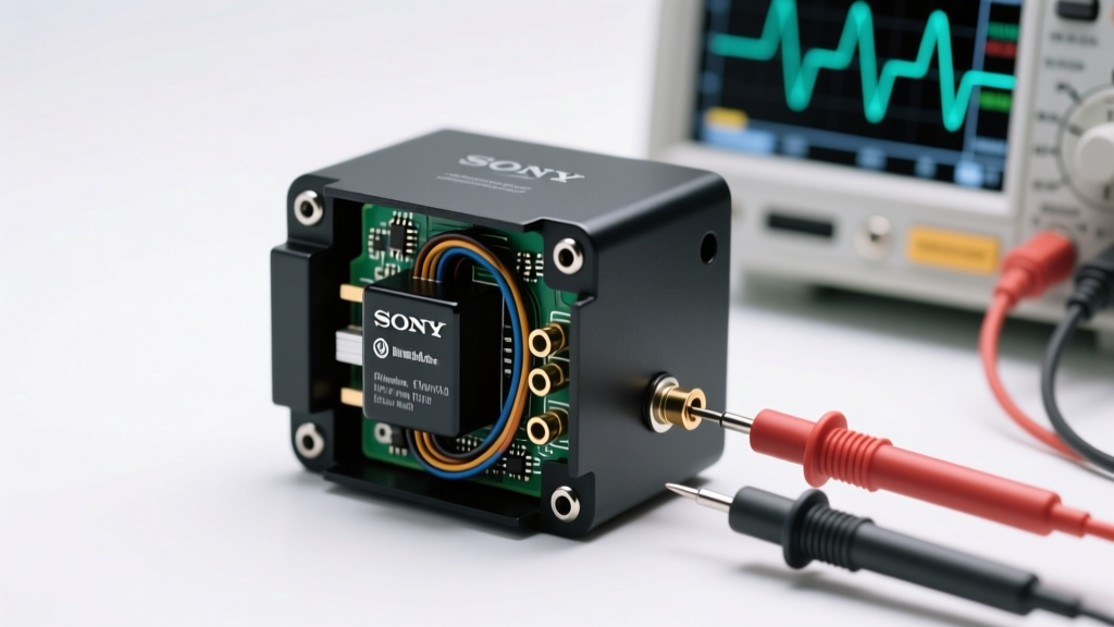
Intel JS28F128P33B85A Flash Memory: Comprehensive Overview
The Intel JS28F128P33B85A is a high-performance flash memory device from Intel's renowned StrataFlash® family. As a 128 Megabit (16MB) non-volatile memory chip, it delivers reliable, low-power data storage for mission-critical applications in networking, telecommunications, and embedded computing systems. Engineered for durability and efficiency, this device excels at storing firmware, boot code, and configuration data, maintaining data integrity across extensive read/write cycles and power cycles.
Key Advantage: The JS28F128P33B85A combines high density with excellent endurance, making it ideal for systems requiring frequent firmware updates and long-term data retention without battery backup.
Memory Architecture
Built on advanced CMOS technology, the JS28F128P33B85A features a sophisticated memory cell matrix that supports multi-bit programming, maximizing its 128Mb storage capacity. Its intelligent architecture includes a flexible partitioning system that allows the memory space to be divided into multiple, independently managed regions.
This capability enables optimized storage management for different data types—such as separating boot code, application firmware, and user configuration settings—enhancing system organization and security.
Performance & Speed
The device delivers exceptional performance with high-speed read operations up to 85 Mbps, ensuring rapid access to critical system code during boot-up and runtime. It supports page programming of up to 32 bytes per cycle, streamlining data writes and reducing programming time.
With multi-bank architecture, the JS28F128P33B85A enables concurrent operations—allowing one bank to be read while another is being programmed or erased. This parallel processing significantly boosts overall system efficiency and responsiveness in real-time applications.
Endurance & Data Retention
Designed for long-term reliability, the JS28F128P33B85A boasts an impressive endurance of up to 100,000 (10⁵) write-erase cycles per sector. This makes it highly suitable for environments with frequent firmware updates or logging operations.
Data integrity is further ensured through exceptional data retention of up to 20 years under standard operating conditions. Even after extended periods without power, stored information remains intact, minimizing the risk of data loss in embedded and industrial systems.
Applications & Use Cases
The robust feature set of the JS28F128P33B85A makes it a preferred choice for storing critical system code in a wide range of advanced electronic devices, including:
- Networking Equipment: Routers, switches, and firewalls requiring secure and updatable firmware
- Telecommunications: Base stations, PBX systems, and communication gateways
- Automotive Systems: Infotainment units, instrument clusters, and ADAS (Advanced Driver Assistance Systems)
- Industrial & Embedded: PLCs, HMI devices, and medical equipment
| Specification | Details |
|---|---|
| Memory Type | StrataFlash® NOR Flash |
| Capacity | 128 Megabit (16MB) |
| Read Speed | Up to 85 Mbps |
| Page Programming | 32 bytes per cycle |
| Write-Erase Endurance | 100,000 cycles (10⁵) |
| Data Retention | Up to 20 years |
| Operating Voltage | 3.3V (typical) |
| Key Features | Multi-bank operation, flexible partitioning, low power consumption |
Design Tip: When integrating the JS28F128P33B85A into embedded systems, leverage its multi-bank functionality to implement wear-leveling algorithms and background firmware updates, maximizing lifespan and system uptime.
Industry Applications of the JS28F128P33B85A Flash Memory Device
The JS28F128P33B85A is a high-performance 128Mb (16MB) flash memory device manufactured using advanced process technology, designed for reliability, endurance, and fast data access. Its robust architecture and extended temperature range make it ideal for mission-critical applications across multiple industries. Below is a detailed exploration of its key industry applications, highlighting how its features address specific operational demands.
Telecommunications
In the telecommunications sector, the JS28F128P33B85A plays a vital role in storing firmware, boot code, and configuration data within network infrastructure equipment such as routers, switches, and base stations. Fast read and programming speeds are essential for minimizing downtime during firmware updates and system reboots—critical in maintaining uninterrupted service.
Its high endurance (capable of withstanding numerous write/erase cycles) and long data retention (up to 100 years under normal conditions) ensure consistent performance over the lifespan of telecom hardware. This reliability reduces maintenance costs and enhances service availability, making it a trusted choice for carriers and service providers managing large-scale networks.
Networking
Modern networking devices—including enterprise-grade routers, managed switches, and firewalls—rely on the JS28F128P33B85A for secure and efficient storage of operating systems, security policies, and real-time configuration files. The device’s multi-bank architecture enables concurrent read and program operations, allowing one bank to execute code while another is being updated—crucial for zero-downtime upgrades in high-availability environments.
With support for rapid data access and reliable performance under continuous operation, this flash memory ensures that network devices can respond quickly to traffic demands and security threats. Its resistance to electrical noise and stable operation across varying temperatures further enhances its suitability for data centers and edge networking applications.
Automotive
Within the automotive industry, the JS28F128P33B85A is deployed in advanced electronic systems such as Advanced Driver Assistance Systems (ADAS), infotainment units, and digital instrument clusters. These systems require non-volatile memory that can reliably store operating software, calibration data, and user preferences—even in harsh environmental conditions.
Designed to operate across an extended temperature range (typically -40°C to +85°C or higher), the device meets automotive-grade reliability standards. Its ability to endure vibration, thermal cycling, and electromagnetic interference makes it ideal for use in vehicles where safety and uptime are paramount. Additionally, its fast boot times contribute to improved user experience in infotainment and navigation systems.
Industrial Automation
In industrial settings, the JS28F128P33B85A is widely used in Programmable Logic Controllers (PLCs), Human-Machine Interfaces (HMIs), and industrial PCs. These systems demand durable, long-lasting memory capable of handling frequent program updates, logging operations, and real-time control data storage.
The device’s high write endurance and resistance to environmental stressors—such as dust, moisture, and wide temperature fluctuations—make it well-suited for factory floors and remote installations. Its predictable performance ensures consistent machine operation, reducing the risk of unplanned downtime and supporting Industry 4.0 initiatives that rely on seamless data flow and edge computing.
Consumer Electronics
The JS28F128P33B85A also finds application in consumer electronics such as smart TVs, set-top boxes, digital media players, and home networking devices. In these products, it stores firmware, application data, and user settings, enabling quick startup times and smooth multimedia experiences.
With a 128Mb capacity, it provides sufficient space for embedded operating systems and essential apps without requiring costly high-density memory solutions. Its low power consumption and compact form factor align well with the design constraints of modern consumer devices, where energy efficiency and miniaturization are key priorities.
Cross-Industry Advantages
Across all these sectors, the JS28F128P33B85A offers several universal benefits:
- High Endurance: Supports up to 100,000 program/erase cycles, ideal for applications requiring frequent updates.
- Long Data Retention: Maintains data integrity for up to 100 years, ensuring longevity in embedded systems.
- Fast Access Times: Enables rapid booting and responsive system performance.
- Extended Temperature Range: Operates reliably in extreme environments, from freezing outdoor installations to hot engine compartments.
- Multi-Bank Architecture: Allows simultaneous read and write operations, improving system efficiency.
| Industry | Primary Use Case | Key Benefit of JS28F128P33B85A |
|---|---|---|
| Telecommunications | Firmware & configuration storage in routers and switches | Reliable updates and long-term data retention |
| Networking | Boot code and OS storage in firewalls and switches | Concurrent operations via multi-bank architecture |
| Automotive | ADAS and infotainment system memory | Extended temperature operation and high reliability |
| Industrial | Data logging and control in PLCs and HMIs | Durability and resistance to harsh environments |
| Consumer Electronics | Media storage and settings in smart TVs and players | Cost-effective 128Mb capacity with fast access |
Note: When integrating the JS28F128P33B85A into any system, always adhere to manufacturer-recommended voltage levels, programming algorithms, and environmental specifications. Proper circuit design—including decoupling capacitors and ESD protection—is essential to maximize device lifespan and prevent premature failure. Consult the official datasheet for timing diagrams, pin configurations, and compliance information.
Product Specifications and Features
The JS28F128P33B85A is a high-performance flash memory chip designed for embedded systems, industrial applications, and firmware storage. As a member of the StrataFlash family, it offers reliable non-volatile storage with robust environmental tolerance and efficient parallel interface communication. This guide provides comprehensive details on its specifications, installation process, and best practices for long-term usage and maintenance.
Key Features and Technical Specifications
Below is a detailed breakdown of the JS28F128P33B85A's core technical attributes, making it suitable for a wide range of demanding applications where durability, stability, and performance are critical.
| Specification | Details |
|---|---|
| Memory Size | 128 Megabits (16 Megabytes) |
| Memory Type | Flash Memory, StrataFlash™ Technology |
| Interface Type | Parallel Interface (8-bit or 16-bit mode support) |
| Operating Voltage | 3.0 V to 3.6 V (Single Power Supply) |
| Temperature Range | Industrial Grade: -40°C to +85°C |
| Package Type | Plastic Leaded Chip Carrier (P-LCC-32) |
| Package Dimensions | 9.7 mm × 12.7 mm × 3.5 mm (L × W × H) |
| Memory Organization | Multiple sectors for flexible erase operations |
| Endurance | Typically 100,000 program/erase cycles per sector |
| Data Retention | Up to 10 years at rated temperature |
| Mounting | Surface Mount (SMD), Reflow Soldering Compatible |
Note: The StrataFlash architecture enables multi-level cell (MLC) operation, allowing two bits per cell in select modes, enhancing effective storage density while maintaining compatibility with standard flash command sets.
How to Install the JS28F128P33B85A Chip
Proper installation is essential to ensure electrical connectivity, thermal stability, and long-term reliability. Follow these step-by-step instructions carefully, especially when working with sensitive surface-mount components.
1. Access the Device Area
Begin by powering down the host device and disconnecting all power sources. Depending on the application, you may need to open an enclosure, remove shielding, or disassemble part of the circuit assembly to access the target location. Ensure electrostatic discharge (ESD) protection is in place—use an anti-static wrist strap and work on a grounded mat.
2. Prepare the Slot/Bay
If replacing an existing memory chip, carefully desolder the old component using a rework station or hot air gun, ensuring no damage to surrounding traces or pads. Clean the landing area with isopropyl alcohol and inspect for solder bridges or debris. Confirm that the footprint matches the P-LCC-32 package dimensions and pin layout.
3. Insert the Chip
Align the JS28F128P33B85A precisely with the PCB footprint, observing correct orientation (typically indicated by a notch or dot on the package). Gently place the chip without applying pressure. Use a fine-tip soldering iron or reflow oven to solder all leads, ensuring consistent joints and avoiding cold solder or shorts. Inspect under magnification if possible.
4. Secure the Device
Once the chip is properly mounted and soldered, allow the board to cool completely. Reassemble the housing or enclosure, ensuring all fasteners are tightened securely and no internal components are strained. Verify that airflow and thermal management remain unobstructed.
5. Power Up and Configure
Reconnect power and boot the system. Enter the BIOS, bootloader, or diagnostic mode to verify that the memory chip is detected. If programming firmware or data, use compatible tools (e.g., JTAG, ISP programmers) and follow the manufacturer's command protocol. Test read/write functionality and confirm stable operation under load.
Professional Tip: Always refer to the official datasheet and application notes from the manufacturer before installation. Consider using automated optical inspection (AOI) or X-ray inspection for critical or high-volume deployments to ensure solder joint integrity.
Usage and Product Maintenance Best Practices
To maximize the lifespan and reliability of the JS28F128P33B85A, follow these recommended maintenance strategies, particularly in industrial, automotive, or mission-critical environments.
Regular Backups
Always maintain regular backups of data stored on the flash chip, especially firmware, configuration files, or calibration data. Use automated backup routines or version control systems to prevent data loss due to unexpected failures. Store backups in separate physical or cloud-based locations for redundancy.
Avoid Excessive Programming/Erasing
While the chip supports up to 100,000 program/erase cycles, frequent writes can accelerate wear. Implement wear-leveling algorithms in firmware when possible, and minimize unnecessary updates. For logging applications, buffer data in RAM before writing in batches to reduce flash wear.
Check for Firmware Updates
Monitor the manufacturer’s website for updated firmware or driver patches that may improve performance, security, or compatibility. Even though the chip itself is passive storage, the controlling software or microcontroller may benefit from updates that optimize interaction with the flash memory.
Monitor Device Health
Use diagnostic tools or built-in commands (e.g., CFI - Common Flash Interface) to monitor chip health. Track parameters such as erase count, error rates, and bad block accumulation. Early detection of degradation allows for proactive data migration and prevents sudden system failures.
Enable Error Correction (ECC)
If supported by the host controller, enable Error-Correcting Code (ECC) features to detect and correct bit errors caused by voltage fluctuations, radiation, or aging cells. ECC significantly improves data integrity, especially in harsh environments or long-term deployments.
Longevity Tip: Store unused JS28F128P33B85A chips in anti-static bags within a temperature-controlled, low-humidity environment. Avoid exposure to direct sunlight, corrosive gases, or strong electromagnetic fields to preserve component integrity before installation.
Q & A: JS28F128P33B85A Flash Memory Chip
Welcome to our comprehensive FAQ guide on the JS28F128P33B85A, a high-performance flash memory solution widely used in mission-critical applications. This guide provides detailed answers to common technical questions about its functionality, durability, and industrial applications. Whether you're an engineer, procurement specialist, or embedded systems designer, this resource will help you understand the key advantages and specifications of this advanced memory device.
Quick Fact: The JS28F128P33B85A is part of Intel’s StrataFlash family, known for delivering reliable, high-speed non-volatile memory performance in demanding environments such as automotive control units and network infrastructure equipment.
Q. What is the primary use of the JS28F128P33B85A?
The JS28F128P33B85A is a 128-megabit (16MB) flash memory chip designed for embedded applications that require fast, reliable, and non-volatile data storage. Its primary use includes storing firmware, boot code, configuration settings, and system parameters in devices where power efficiency and data integrity are critical. Due to its robust architecture and industrial temperature range support, it is widely deployed in telecommunications equipment (such as routers and switches), networking hardware, automotive electronics (including engine control units and infotainment systems), and industrial automation controllers.
Q. How does the JS28F128P33B85A compare to traditional hard drives for storing critical data?
Unlike traditional hard disk drives (HDDs), which rely on mechanical components like spinning platters and moving read/write heads, the JS28F128P33B85A is a solid-state flash memory device with no moving parts. This fundamental difference offers several key advantages:
- Faster Access Times: Enables near-instantaneous data retrieval, crucial for real-time system booting and operation.
- Higher Shock and Vibration Resistance: Ideal for rugged environments such as automotive and industrial applications.
- Lower Power Consumption: Reduces energy usage and heat generation, making it suitable for compact and battery-powered systems.
- Smaller Form Factor: Saves valuable board space in densely packed electronic assemblies.
- Improved Reliability: Eliminates mechanical failure risks associated with HDDs, significantly reducing downtime and maintenance needs.
These features make the JS28F128P33B85A a superior choice for applications requiring compact, durable, and high-speed storage of critical data.
Q. How many times can the JS28F128P33B85A be written and erased?
The JS28F128P33B85A is engineered for endurance and can typically withstand up to 100,000 program/erase (P/E) cycles per sector. This level of durability makes it significantly more resilient than earlier generations of flash memory and suitable for dynamic environments where firmware updates, logging, or frequent configuration changes occur. Advanced wear-leveling techniques in host controllers further extend its operational lifespan by distributing write operations evenly across memory blocks, minimizing localized wear and maximizing long-term reliability.
Note on Longevity: While 100,000 cycles represent a typical specification under standard conditions, actual endurance may vary based on operating temperature, voltage stability, and access patterns. For mission-critical systems, it's recommended to implement monitoring and redundancy strategies to ensure continued data integrity over time.
Q. What type of technology is used in the JS28F128P33B85A?
The JS28F128P33B85A leverages Intel’s StrataFlash™ technology, a multi-level cell (MLC) flash architecture that stores multiple bits per memory cell without sacrificing speed or reliability. This technology enables higher storage density and cost efficiency compared to single-level cell (SLC) alternatives, while still maintaining excellent performance for code execution and data storage. Key features include:
- High-speed random access for fast boot-up and real-time processing
- Low-latency read operations ideal for executing code directly from flash (XIP – eXecute In Place)
- Support for both buffered and unbuffered interfaces for flexible integration
- Advanced command sets for sector protection, suspend/resume programming, and software locking
StrataFlash technology strikes an optimal balance between performance, capacity, and cost, making it ideal for embedded systems that demand efficient and scalable memory solutions.
Q. What industries benefit most from using the JS28F128P33B85A?
The JS28F128P33B85A is particularly valued across several high-reliability industries due to its combination of speed, durability, and environmental resilience:
| Industry | Key Applications | Why JS28F128P33B85A Excels |
|---|---|---|
| Telecommunications | Routers, switches, base stations | Fast boot times, reliable firmware storage, resistance to vibration and temperature extremes |
| Networking | Firewalls, gateways, network-attached storage (NAS) | Durable configuration storage, low-latency access, compact footprint |
| Automotive | ECUs, ADAS systems, infotainment units | Wide operating temperature range (-40°C to +85°C), high reliability, long-term data retention |
| Industrial Automation | PLCs, HMIs, sensors, robotics | Resistance to shock, dust, and electrical noise; endurance for frequent updates |
| Military & Aerospace | Avionics, communication systems, ruggedized computing | Proven reliability in extreme conditions, secure data storage capabilities |
Design Tip: When integrating the JS28F128P33B85A into your system, ensure proper PCB layout practices—such as minimizing trace lengths, using decoupling capacitors, and adhering to datasheet-recommended voltage tolerances—to maximize signal integrity and long-term performance.
In summary, the JS28F128P33B85A stands out as a versatile and dependable flash memory solution for engineers designing robust embedded systems. Its advanced StrataFlash technology, high endurance, and broad industrial applicability make it a trusted component in applications where failure is not an option. Always refer to the official Intel datasheet and application notes for detailed electrical specifications, timing diagrams, and integration guidelines.